General Description
This document provides information on the function and use of the RTQ6056 evaluation board (EVB), as well as instructions for operating and modifying the board and circuit to meet individual requirements. Additionally, it includes details on the schematic diagram, bill of materials, and evaluation board layout.
Performance Specification Summary
Summary of the RTQ6056GF Evaluation Board performance specificiaiton is provided in Table 1. The ambient temperature is 25°C.
Table 1. RTQ6056GF Evaluation Board Performance Specification Summary
|
Specification
|
Test Conditions
|
Min
|
Typ
|
Max
|
Unit
|
|
Default Input Voltage
|
Default = 12V
|
0
|
--
|
36
|
V
|
|
Supply Voltage
|
Default = 3.3V
|
2.7
|
--
|
5.5
|
V
|
|
Sensing Current
|
|
--
|
0.5
|
--
|
A
|
|
1 LSB Step Size
|
Sense voltage
|
--
|
2.5
|
--
|
μV
|
|
Bus voltage
|
--
|
1.25
|
--
|
mV
|
|
Quiescent Current
|
TA = 25oC
|
--
|
550
|
650
|
μA
|
|
Shutdown mode
|
--
|
3.5
|
6
|
μA
|
Power-up Procedure
Suggestion Required Equipments
- DC Power Supply (Chroma, 62006P-100-25)
- Electronic load capable of 6A
- DC Meter
- Richtek Wrenboard
Quick Start Procedures
1. Apply VS = 3.3V input power supply (2.7V < VS < 5.5V) to VS and GND terminals.
2. Apply 12V input power voltage (0V < IN+ < 36V) to IN+ and GND terminals.
3. The default sense resistance is 100mΩ.
4. Connect an external load to IN- and GND terminals, and keep loading current = 0.5A.
5. Measure the sense voltage (approximately 50mV) between IN+ and IN-.
6. Use RTQ6056 GUI to check practical sense voltage, bus voltage, current and power.
Graphical User Interface
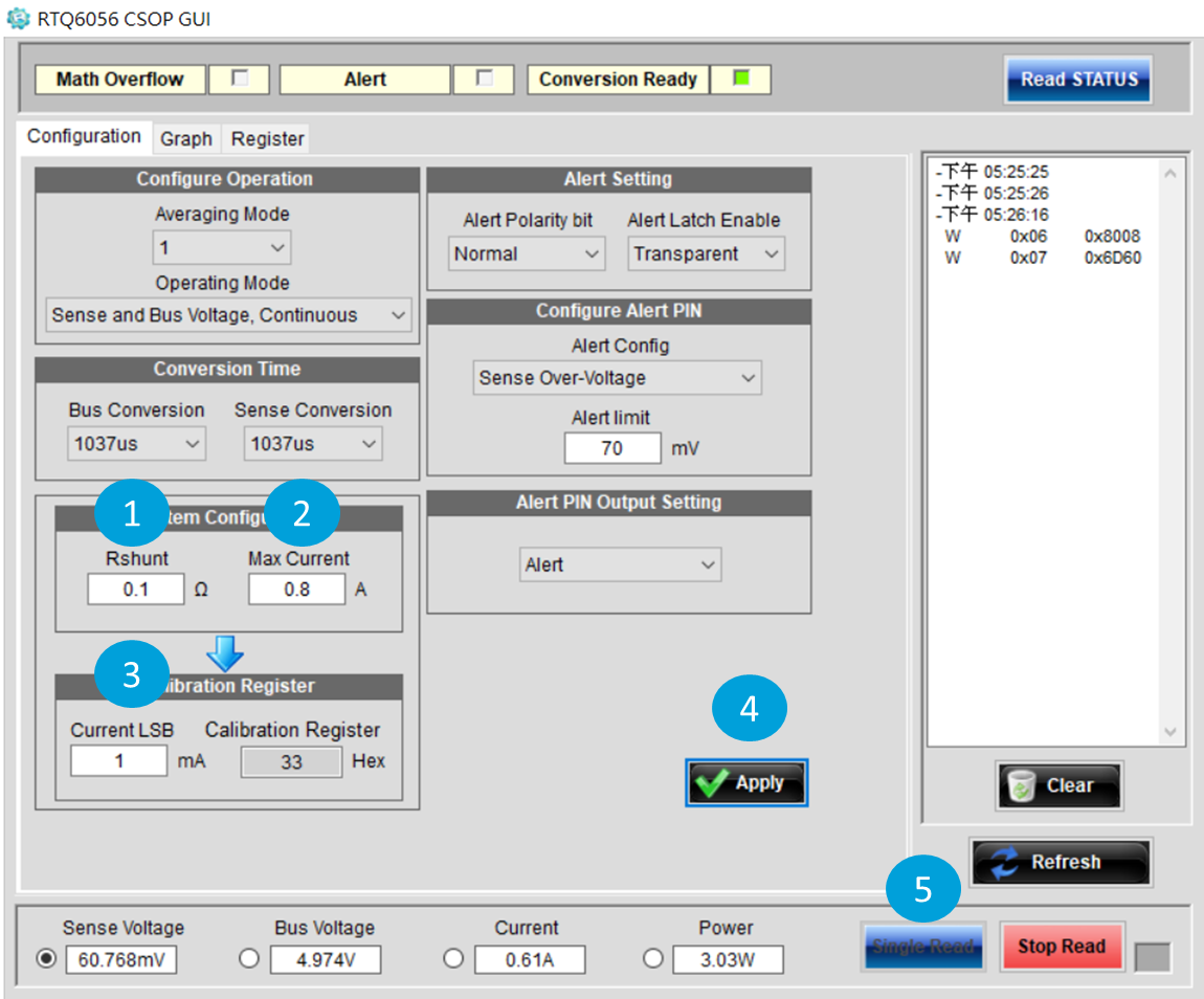
Figure 1. RTQ6056 Graphical User Interface
Configuring the RTQ6056 EVB Software
Step 1. Set the shunt resistor value.
Step 2. Set Max expected current for sensing.
Step 3. Set minimum current resolution for current LSB.
Step 4. Push “Apply” bottom, the 0x05 Calibration register is written into a value for expected current LSB.
Step 5. Select single read or continued read for showing practical data.
Alert Indicator
Figure 2 shows an example for configuring the Alert pin. The user can monitor five alert functions or conversion ready notification through the alert config drop-down menu, and the threshold can be programed in the Alert Limit.
The five alert functions are listed below:
- Sense Voltage Over-Limit (SOL)
- Sense Voltage Under-Limit (SUL)
- Bus Voltage Over-Limit (BOL)
- Bus Voltage Under-Limit (BUL)
- Power Over-Limit (POL)
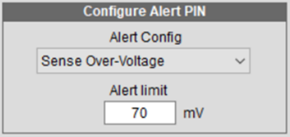
Figure 2. Configuring the Alert Pin
Detailed Description of Hardware
Headers Description and Placement
Carefully inspect all the components used in the EVB according to the following Bill of Materials table, and then make sure all the components are undamaged and correctly installed. If there is any missing or damaged component, which may occur during transportation, please contact our distributors or e-mail us at evb_service@richtek.com.
Test Points
The EVB is provided with the test points and pin names listed in the table below.
|
Test Point/
Pin Name
|
Function
|
|
A1, A0
|
Slave address selection
|
|
IN+
|
Positive current-sensing input.
|
|
IN-
|
Negative current-sensing input.
|
|
VBUS
|
Bus voltage input.
|
|
VS
|
Power supply, 2.7V to 5.5V
|
|
Alert
|
Multi-functional alert, open-drain output.
|
Bill of Materials
|
|
VIN = 12V, VS = 3.3V, IOUT = 0.5A
|
|
|
Reference
|
Count
|
Part Number
|
Value
|
Description
|
Package
|
Manufacturer
|
|
U1
|
1
|
RTQ6056GF
|
RTQ6056GF
|
16-Bit ADC Op Amp
|
MSOP-10
|
RICHTEK
|
|
C1, C2, C5, C6
|
4
|
GRM188R71H104KA93D
|
0.1µF
|
Capacitor, Ceramic, 50V/X7R
|
0603
|
MURATA
|
|
R1, R2
|
2
|
RAT030000FTP
|
0/0603
|
Resistor
|
0603
|
RALEC
|
|
R5
|
1
|
WR06X1002FTL
|
10k/0603
|
Resistor
|
0603
|
WALSIN
|
|
RSEN1
|
1
|
RTT25R100FTE
|
0.1/2512
|
Resistor
|
2512
|
RALEC
|
|
|
|
|
|
|
|
|
Typical Applications
EVB Schematic Diagram
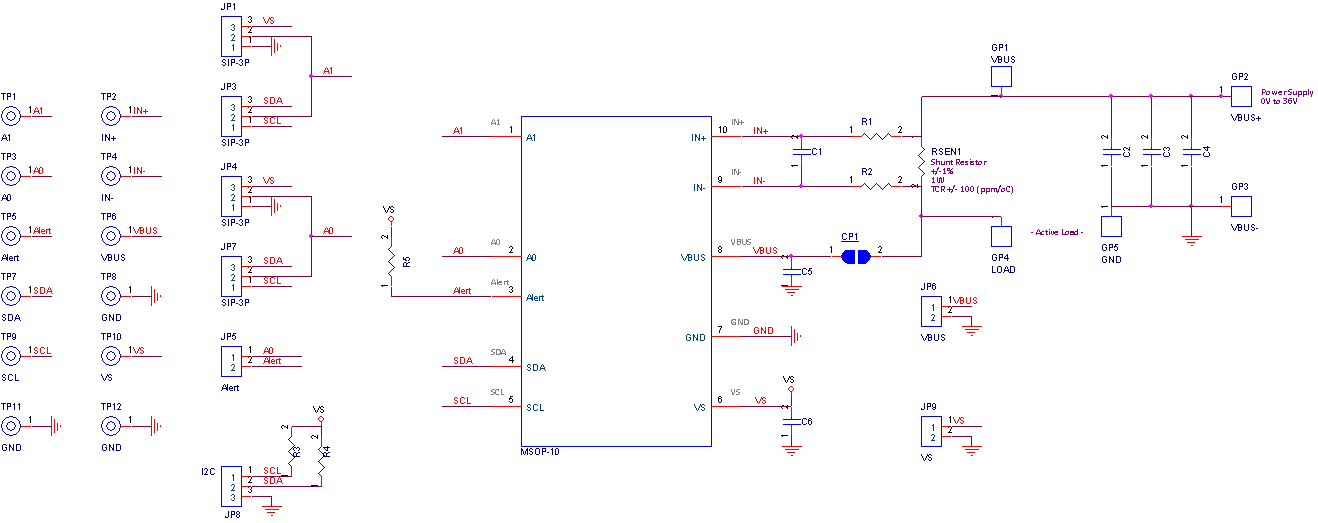
1. The capacitance values of the input and output capacitors will influence the input and output voltage ripple.
2. MLCC capacitors have degrading capacitance at DC bias voltage, and especially smaller size MLCC capacitors will have much lower capacitance.
Measurement Results
|
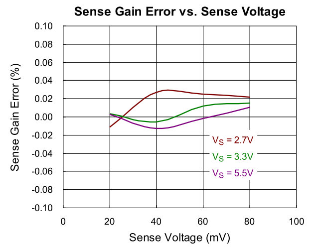
Sense Gain Error with Power Supply Measurement
|
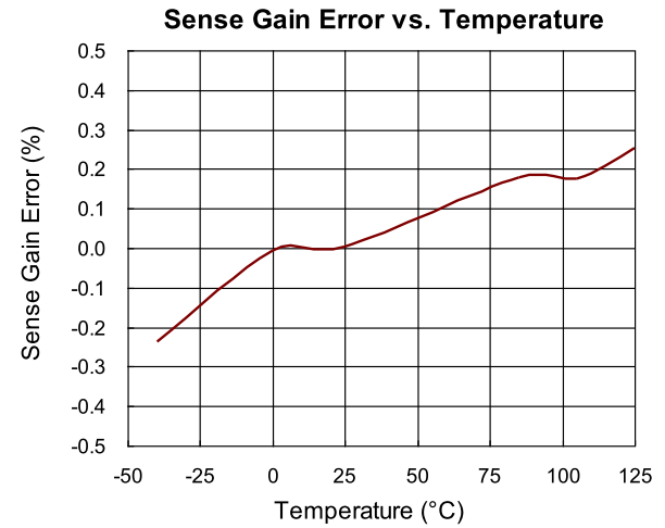
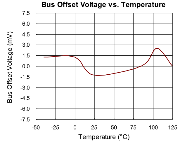
Sense Gain Error with Temperature Measurement
|
|
|
|
|
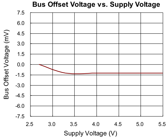
Bus Gain Error with Power Supply Measurement
|
Bus Gain Error with Temperature Measurement
|
|
|
|
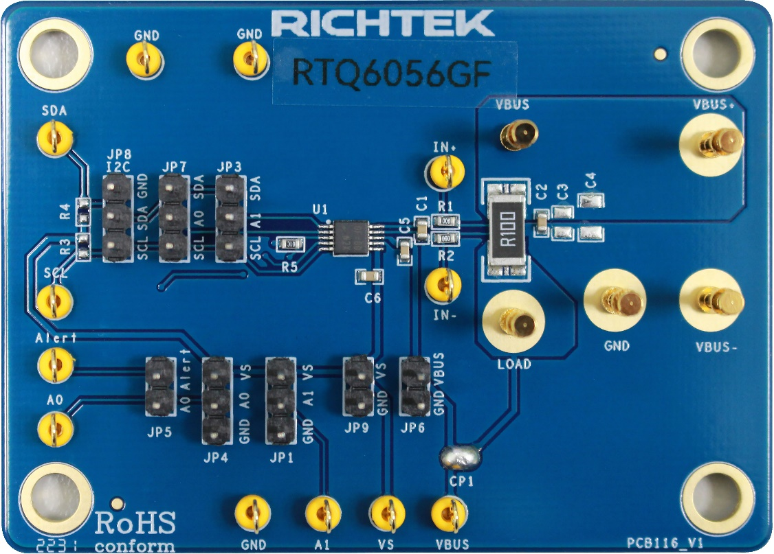
Evaluation Board Layout
Figure 3 and Figure 4 are RTQ6056GF Evaluation Board layout. This board size is 70mm x 50mm and is constructed on two-layer PCB, outer layers with 2 oz. Cu and inner layers with 1 oz. Cu.
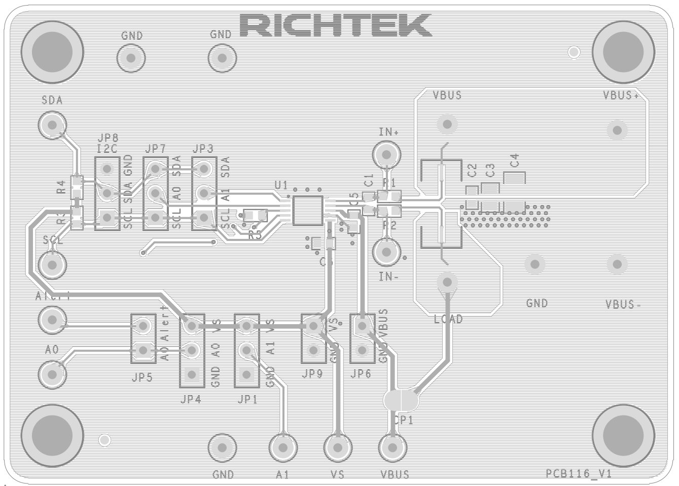
Figure 3. Top View
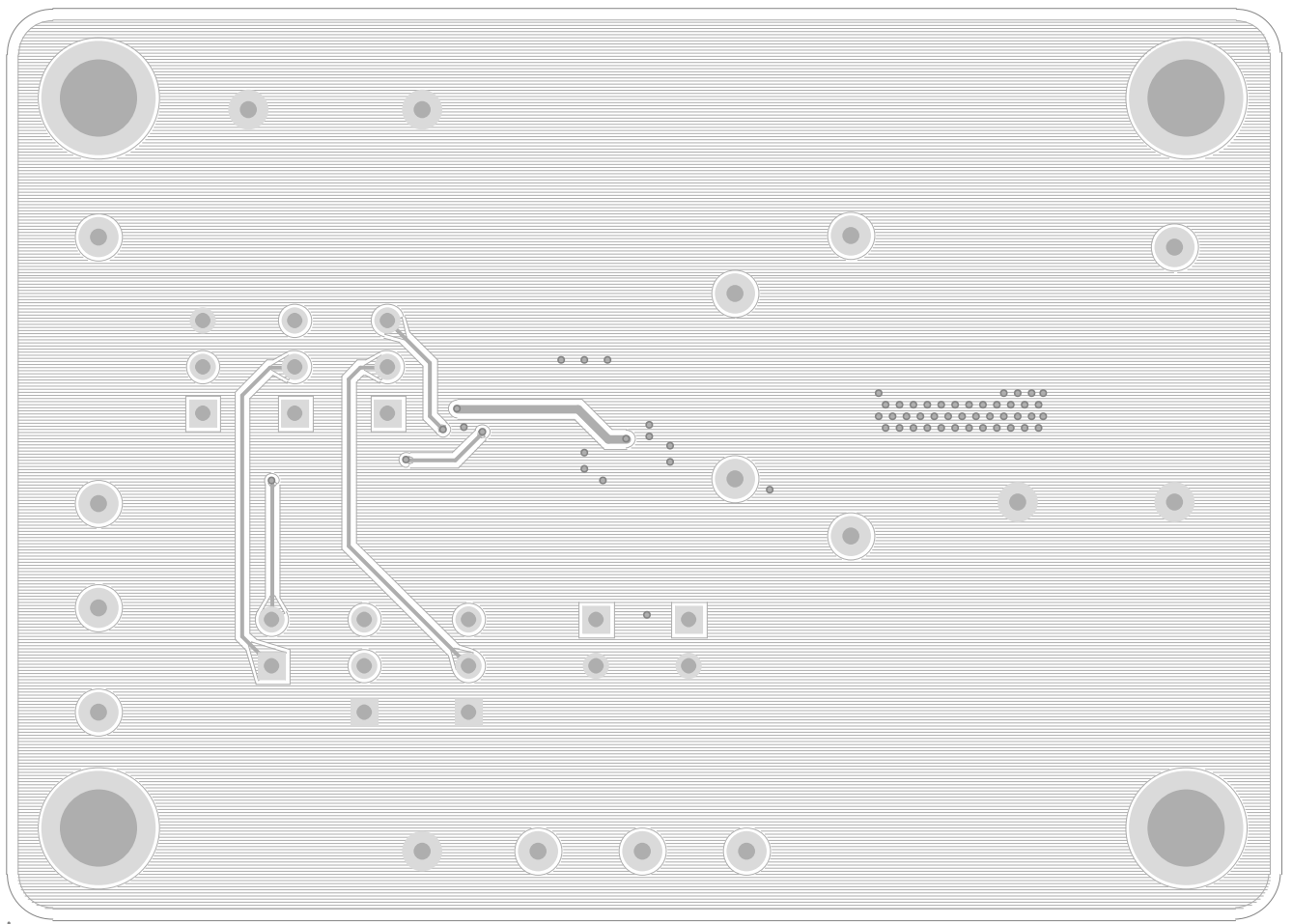
Figure 4. Bottom View